The Basics of Soldering — Part 2
By Bob Wettermann, Nick Brucks View In Digital Edition
While SMT (surface-mount technology) components are the predominant type of package today, there still remain many through-hole components that must be soldered on most mixed technology projects. This is typically because these components have a better mechanical rigidity for interaction with your project, or for higher voltage components such as some power transistors or capacitors.
There are a variety of materials required for the through-hole soldering of axial leaded components. For this type of placement and soldering, the following tools and components are required:
- Printed circuit board (PCB)
- Wire solder
- Flux
- Axial leaded components
- Alcohol
- Soldering iron with chisel tip
- Pliers (lead forming)
- Acid brush
- Solder wick
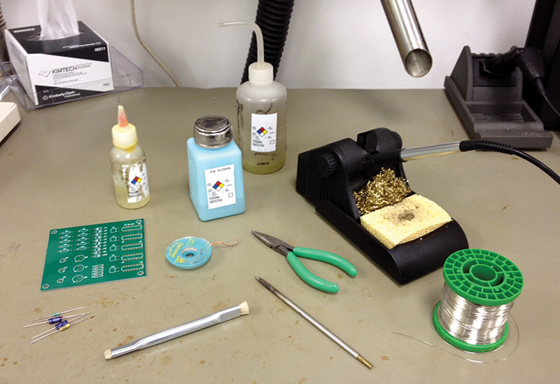
FIGURE 1. Materials.
Before beginning the soldering process, there are a few safety and electrostatic discharge (ESD) precautions one needs to take before soldering components.
Soldering tips get very hot (+445°F!) and therefore are a very painful potential burn hazard to some of the most sensitive parts of your body — your fingers! Always assume the soldering tips are hot! Make sure to wash your hands after soldering prior to eating — especially when soldering with tin-lead soldering systems.
While the safety aspect of soldering has to do with protecting yourself from hot objects and foreign chemicals, the other things that need to be protected are the devices. While the majority of through-hole devices are passive in nature and therefore do not in every case require ESD or MSD controls, it’s always good procedure to make sure you are properly grounded (see Part 1 of the series), and to assume that all components on today’s PCBs can be susceptible to ESD damage events.
There are two component body styles in which the process of hand soldering will be discussed here: a simple through-hole axial leaded component, and a through-hole connector.
Refer to the photos as we discuss the process by which a through-hole axial leaded component is soldered onto a PCB.
1. Clean the component leads with isopropyl alcohol. Use Kimwipe paper tissue with a light wiping action. (CAUTION: DO NOT BEND THE COMPONENT LEADS.) Wipe the component dry to remove alcohol residue. As an option, you may want to tin the soldering tip in order to insure proper wetting of the solder.
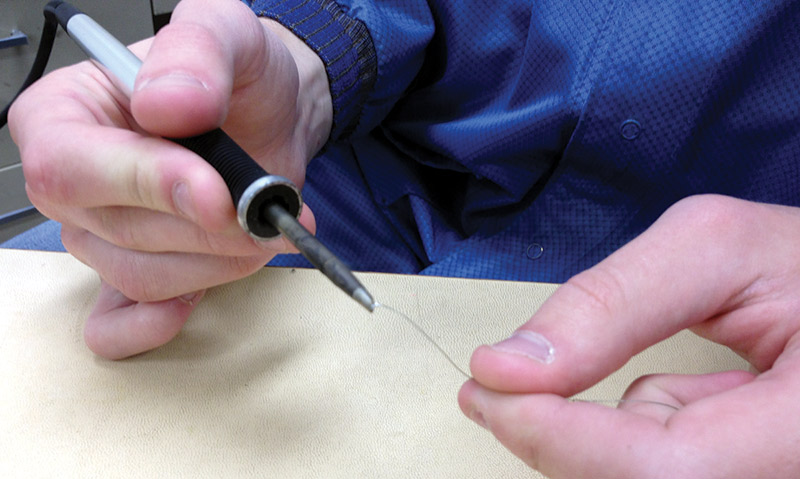
FIGURE 2. Tinning the soldering tip.
2. Prepare the lands and pads for soldering. Clean the pads/lands on the PCB using the alcohol method on both sides of the PCB where the components will be installed. Tin the pad surfaces by flowing solder onto the pads, and then removing it by either wicking or extraction. Remove all excess solder and clean using an acid brush and alcohol. (CAUTION: DO NOT APPLY ANY EXCESSIVE DOWNWARD PRESSURE WHEN WICKING OFF SOLDER FROM THE PADS OR YOU MAY DAMAGE THEM.)
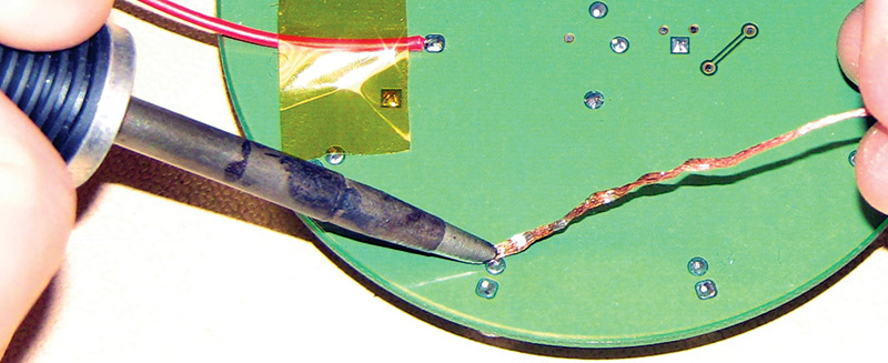
FIGURE 3. Tinning the pads.
3. Place the axial leaded resistor on the component side of the PCB, centering the component body between the PTHs (plated thru-holes) where the resistor will be soldered. Position the edge of the lead forming pliers over the center of the PTH and grip the lead with the pliers. (Hold the lead tight enough so that it will not move when you form the 90 degree bend, but gently enough not to cause lead damage.) Position your thumb or index finger on the component body and push the component body to form a single 90 degree bend. The pliers are strictly used to hold the component lead as all bending action is done with the thumb or finger.
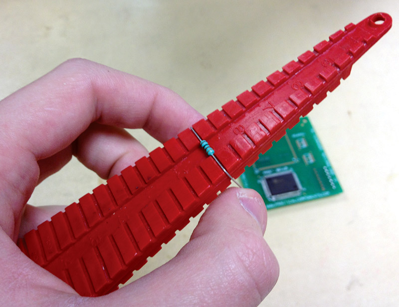
FIGURE 4. Bending the leads of a resistor using a Christmas tree prep tool.
4. Insert the bent side of the component lead into one of the PTHs.
5. Repeat this bending technique for the other side of the resistor.
6. Inspect the component leads. They should fit loosely into the PTHs with two distinct 90 degree bends.
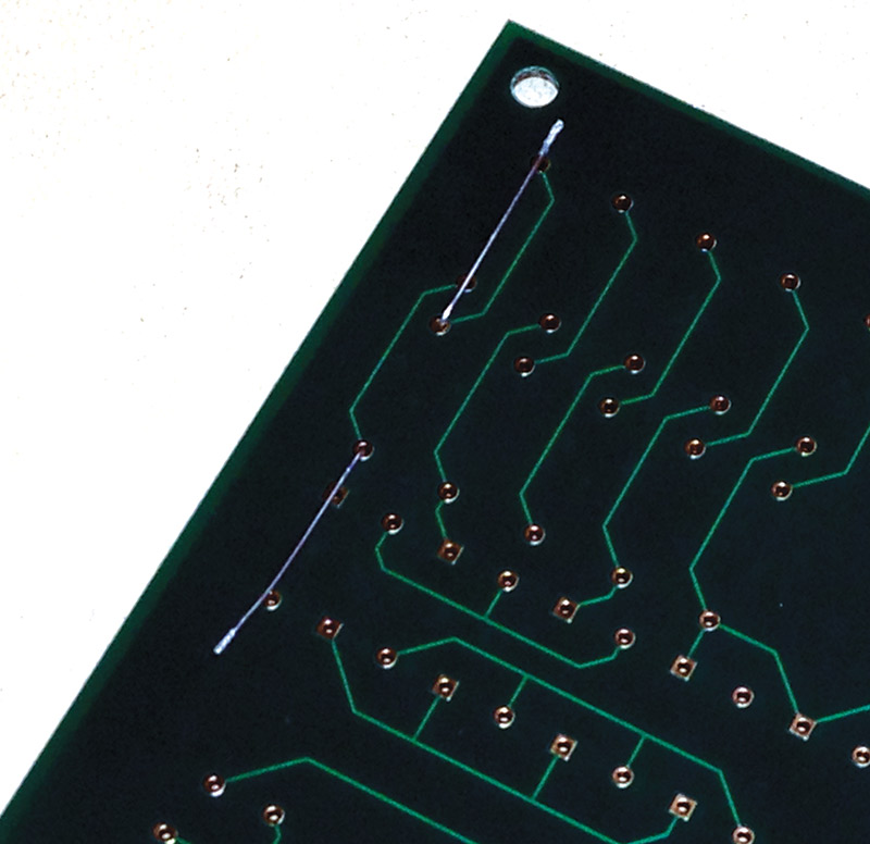
FIGURE 5. The underside of a properly placed component with leads bent down.
7. Ensure the component is flush to the PCB while cutting the end of the leads that are sticking out from the other side of the board. Using cutters, snip the leads to approximately 1.5 mm long. The easiest way to do this is to place a dime — which is approximately 1.3 mm in thickness — at the back from the leads, using it as a guide on where to make the trims. Once the leads have been cut, use a wooden stick to bend the leads down to contact the pad, and hold the component in place. This should be a fully clenched termination which will help to hold the component in place while soldering.
Now that we have the leads clenched and the component held in place, you can begin soldering.
8. Apply flux to both the termination and component sides of the PCB. Flux is an acidic material that is designed to clean oxides from and help transfer heat to the solder joint. (Here’s a quick tip on choosing the correct flux: No-clean flux leaves much less residue. Many manufacturers choose no-clean flux in order to omit the cleaning process after soldering. However, we will still clean the board after soldering. Also know that combining higher tip temperatures and no-clean fluxes will sharply reduce tip life.)
9. Clean and thermal shock the soldering iron tip.
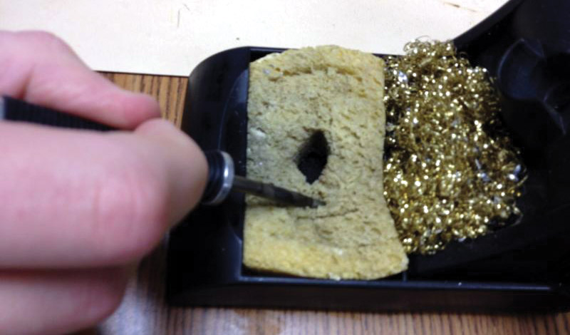
FIGURE 6. Cleaning the tip using a wet sponge.
How to choose the right soldering iron tip:
It is very important to choose the correct tip geometry for the application. The tip must fit the joint correctly. A correct fit will maximize power delivery, increase tip life, and result in higher efficiency. A chisel style of tip will work in most instances. Scratching, rubbing, pressing hard, etc., will not aid in the transfer of heat. Using a tip that is too small will take longer, will abuse the tip, and will not efficiently pass power to the load. A small tip will seem to be too cold or too slow. A tip that is too large will damage the PCB, abuse the tip, and could make a hole in the tip.
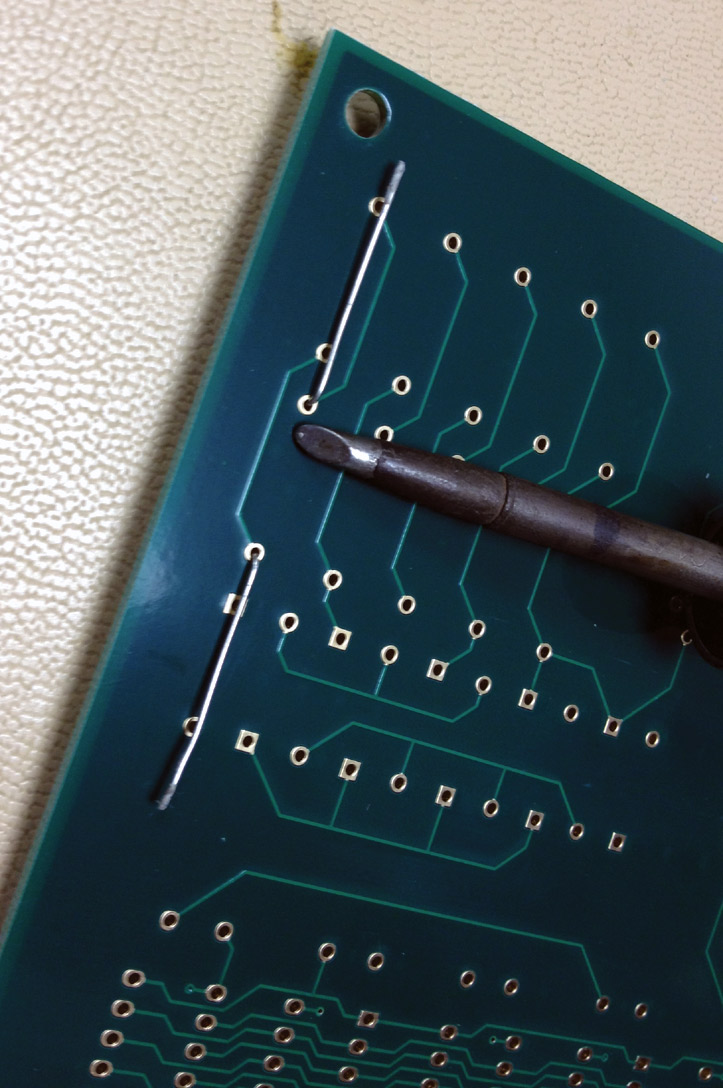
FIGURE 7. Choose the correctly sized solder tip (slightly larger than the pad).
While holding the component in place on the PCB with a heat resistance pad, tack-solder one side of the component lead termination. Place the soldering iron tip at the junction between the pad and component lead. Apply a small amount of solder at the junction of the soldering iron tip and lead to make a solder bridge. For most projects, use a .015” or 0.020” diameter wire flux cored solder. For prototypes, use Sn63Pb37 (or “leaded”) solder as this will wet the solder pads more easily and lower the melting point more quickly.
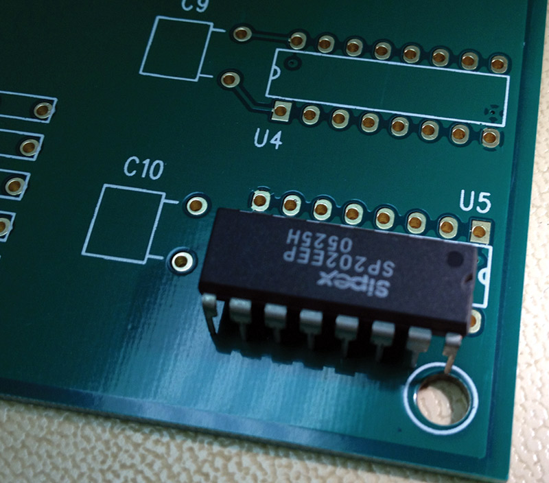
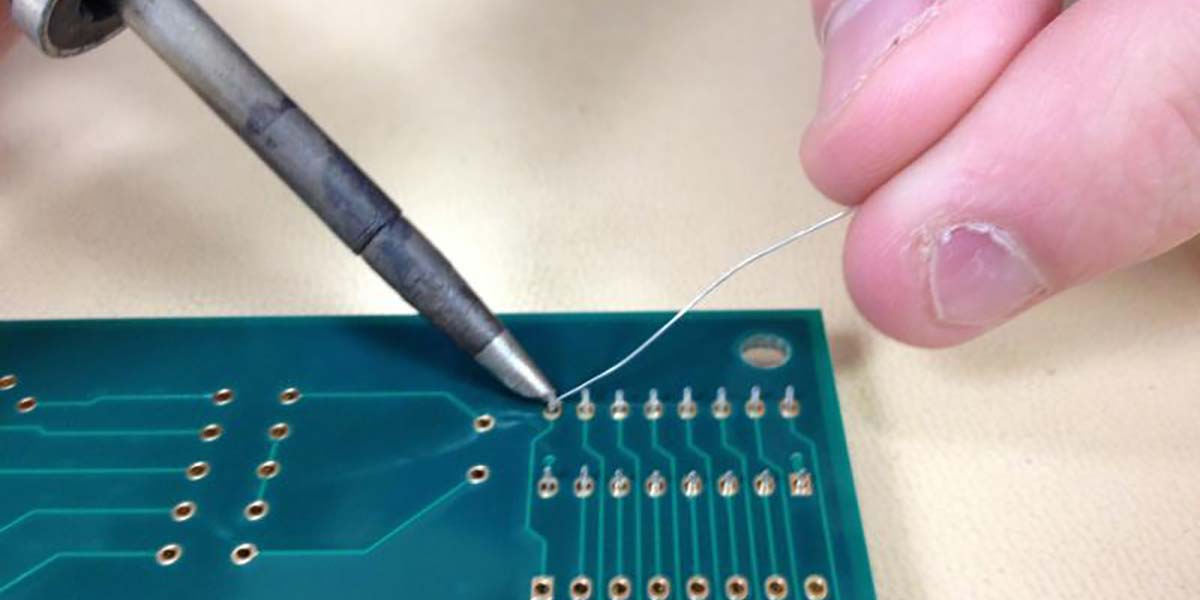
FIGURE 8. Make sure the notch on the DIP matches the correct orientation with the notch on the PCB before soldering.
With the component now held in place by the tack-soldered connection, solder the other lead using the same proper soldering technique.
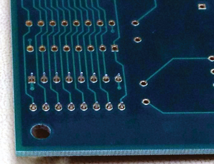
FIGURE 9. Underside view.
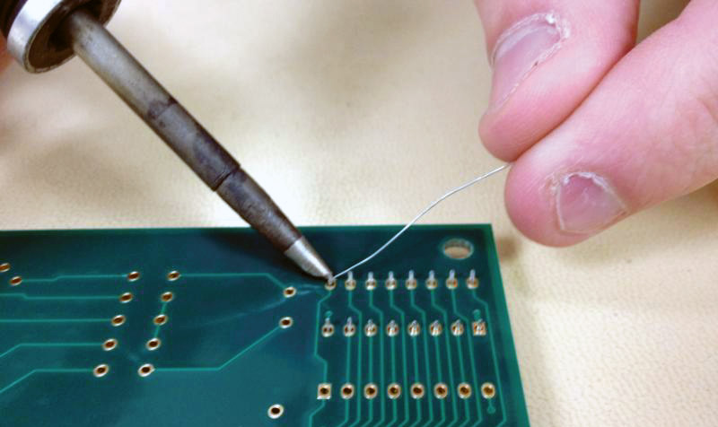
FIGURE 10. Tacking down opposite corners of the DIP to hold it in place.
How to pick the right soldering temperature:
Start with a 340°C soldering iron temperature for the leaded solders (380°C for lead-free SAC alloy solders). If your board is simple and does not have too many backplanes, use this temperature. If you are soldering a heavy board with copper planes, you may want to use a higher temperature series, or use bottom side heating in addition to the soldering iron.
10. Clean both sides of the PCB using the alcohol method.
11. Inspect both sides of the PCB in accordance with IPC-A-610 (the globally preferred international acceptance standard for electronics assembly).
While this is not an all inclusive inspection article, there are some more common “gotchas” that can be a reason for retouching soldering joints:
- Lead bend radius is less than one lead diameter.
- Lead is nicked more than 10% of lead diameter.
- Lead is deformed from repeated bending.
- Fully-clinched lead length on the secondary side of the board is more than 2.5 mm and is bent toward an uncommon electrical trace in the same direction of where the lead came from.
- The circumference of wetting around the lead and pad on the component side of the PCB is less than 180 degrees.
- The circumference of the solder fillet and wetting around the lead and pad on the opposite side of the component is less than 270 degrees.
- On the component termination side, wetting on the land area is less than 75%.
- Solder fillets are not concave in shape and do not have a feathered edge.
The solder joint surfaces should be smooth, nonporous, and look undisturbed, with a finish varying from satin to bright. Make sure that the fillet completely wets all the elements of the connection and is concave.
Another through-hole device type which is often seen on build projects are DIP components. Unlike axial leaded components, these devices do not require a lot of lead preparation, but they do require a higher degree of soldering skill.
The device preparation as well as the materials for the preparations and soldering of these type of components is similar to the previously discussed axial lead termination components. Typically, when handling these devices, the leads — being greater in number — are much more sensitive to any handling damage and precaution should be exercised as they can easily be bent or destroyed.
Here are the steps for soldering a connector into place:
- Clean the contacts. You may want to pretin the contacts in order to insure solderability of the pins.
- Clean pads/lands using the alcohol method on both sides of the PCB where the DIP components will be installed.
- Prepare the component for soldering. Using the lead forming pliers, gently bend the component leads so they all will fit loosely into the holes. Make sure the orientation of the connector is correct with either a pin 1 marking or a silk screen outline of the part imprinted on the PCB.
- Apply liquid flux on all the leads on the opposite side of the PCB.
- Solder-tack the opposite cornered leads in place. Make sure the connector is flush with the board or is all the way anchored to the PCB.
- Solder connections on every other lead, then go back and fill in the leads in between. Do not start the soldering process at the tacked-in place leads as these will be holding the part in place.
- Clean solder connections on both sides of the PCB using alcohol, and blot dry any solvent residue.
- Inspect the component just soldered into place.
While this short article does not afford us the time to talk about all of the acceptance criteria for this kind of a connection, the biggest gotchas for these multi-leaded components to watch out for post-soldering are:
- Incorrect polarity or orientation of the connector.
- Tilt of the connector, resulting in lead protrusion or non-functioning of the connector in the designated housing.
- The lack of cleanliness as seen by visible flux residue or metallic areas exhibiting a crystalline white deposit.
- Circumference of wetting around lead and pad on the component side of PCB is less than 180 degrees.
- Circumference of solder fillet and wetting around the lead and pad on the termination side of PCB is less than 270 degrees.
- Solder filled plated thru-hole less than 75%.
- Plated-thru holes with thermal heatsink plane, solder filled hole less than 50%.
- On the component termination side, wetting on land area less than 75%.
- Solder fillets are convex in shape; no feathered edge apparent.
While only two types of through-hole body styles were shown to be soldered here, similar processes and procedures are applicable to other body styles. In Part 3 of this series, we will go through basic soldering skills for surface-mount devices. SV
Article Comments