Basics of Soldering
By Bob Wettermann, Nick Brucks View In Digital Edition
Roboticists need a plethora of skills to create and construct their automatons. Knowing how to solder is a major part of moving from simple kits into the realm of advanced circuits and chassis. This series of articles will serve as a step-by-step guide to hand soldering electrical components.
This first part will focus on the tools and materials you'll need, the basics of the soldering process, and some terminology that needs to be defined before more specific topics are covered. If you already have some experience with soldering, this will be mostly review.
Electrostatic Discharge (ESD)
Before moving on to the specific topic of soldering, it is first useful to discuss ESD. ESD — or Electrostatic Discharge — is the sudden discharge of static electricity between two objects. We routinely encounter ESD in our daily lives. It’s that shock you feel when you touch your car door in the dry winter months or when you walk across a carpet and then touch a door knob. This charge can be in excess of 20,000 volts — much more than it takes to destroy most electronic components (Figure 1).
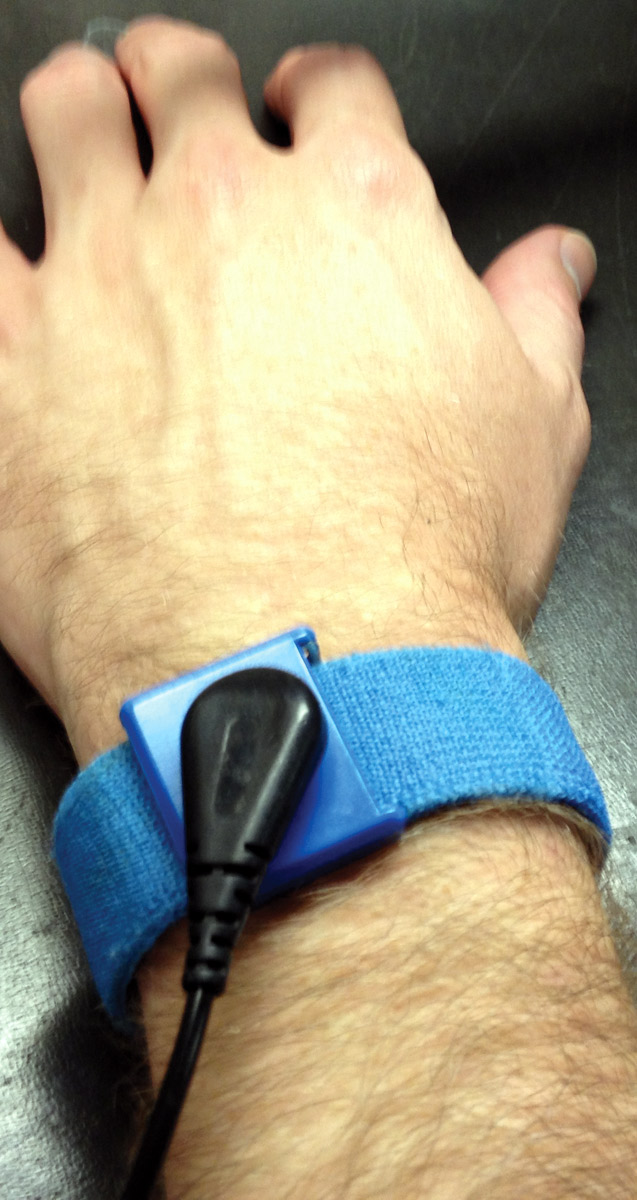
FIGURE 1. Make sure you are properly grounded.
Because of this, preventing an electrical charge from building up is important when working with electronics, since even a small potential can destroy sensitive components.
To avoid building up any excess charge:
- Avoid loose clothing or clothing that dangles down in contact with ESD-sensitive devices
- Wear materials made of cotton, rather than wool or synthetic materials
- Wear a properly grounded ESD wrist strap and/or heel straps, making sure it is properly grounded. You can find these on the Internet at reasonable prices if you’re worried about accidentally damaging components.
In general, it is also good practice to minimize handling of ESD-sensitive devices whenever possible, since the more you handle a device, the more opportunities you have to accidentally damage it with an electrical discharge.
Soldering
Okay, let’s move on to soldering. Soldering is the process of joining two metals together by the use of a solder alloy. It is one of the oldest known joining techniques. The successful soldering process produces a reliable solder connection — one that has both a strong physical bond and electrical connection.
Alloy
The solder alloy utilized is a key material used in the soldering process. Solder used in electronics is a metal alloy. A common alloy is the combination of tin and lead in different proportions for lead bearing solders, and tin, silver, and copper for the lead-free solders. When labeling or naming the different types of solder, manufacturers use the chemical symbols for each of the metals. For example, tin is noted as “Sn,” silver is “Ag,” copper is “Cu,” and lead is “Pb.”
Following this logic, the designation of a common lead-free solder is SAC305. This means that the alloy is made up of 96.5% tin, 3% silver, and 0.5% copper. Knowing what kind of solder alloy you will need to work with is important because different solders will have different melting points and will change the amount of heat you need to liquify the solder quickly.
For example, SN63/PB37 tin-lead solder has a melting point of 361°F (187°C), while some lead-free solders melt at a temperature of approximately 422°F (217°C). With this knowledge, you will be better able to limit the maximum temperature during the soldering operation and minimize the soldering time to make sure you get a reliable solder joint. In addition, it is important not to cross-contaminate lead-bearing and lead-free soldering materials.
Flux
The next thing you’ll need for soldering is flux. Flux is essential to assure solderability and the formation of proper solder joints. The main purposes of flux are:
- To remove surface oxides from the solderable surfaces
- To aid in heat transfer
This will allow the solder to “wet” or stick to the surface better.
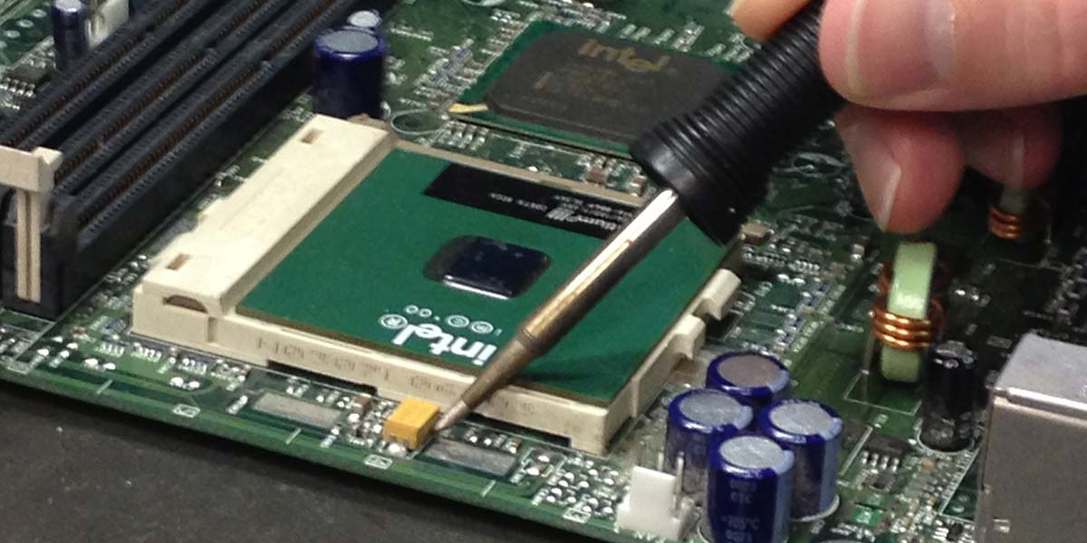
There are primarily two types used for hand soldering operations. The first is rosin flux. Pure rosin flux is weak at room temperature, but reacts strongly with metal oxides at elevated temperatures. That’s why we say that flux is heat activated. The other main type of flux is No-Clean. No-Clean fluxes are made of an entirely different composition compared to rosin fluxes. They are largely composed of organic or inorganic materials with approximately 97% being the carrier (alcohol or water). In conjunction to an external flux application, we also apply flux via the solder wire we use (Figure 2). Solder wire may have either 1.1, 2.2, or 3.3 percent flux by volume in the core of the wire.
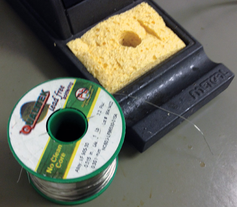
FIGURE 2. Wire cored solder contains flux — make sure you use the right alloy and flux.
Heat
You’ll also want to think about which method you will use to transfer heat when soldering. There are two common types of heating methods used in hand soldering. These types are convective (Figure 3) and conductive (Figure 4).
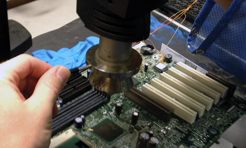
FIGURE 3. Convective soldering is typically used for more complex SMT components.
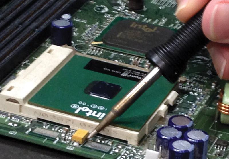
FIGURE 4. Conductive soldering.
The most common method is through conductive soldering. In this method, a soldering iron is used to make contact with the materials to be connected together. This rapidly transfers heat directly to the area, making this the preferred method of hand soldering. To enhance this process, a “heat bridge” composed of a small quantity of liquid solder is formed between the hot soldering iron and the component.
In convective soldering, air is used as the major supplier of heat. For this, you will need a heat gun or similar tool that blows hot air onto the area to be soldered. This method is a less efficient method of heat transfer due to the inability of air to transfer heat quickly. Because of this, when using convective soldering you need to be very careful.
The longer heat is applied to a board, the more likely it is that you could blister/damage the laminate, reflow neighboring parts, or destroy heat-sensitive components of an electronics assembly like glue, batteries, and plastic connectors.
When using a soldering iron, it is important to think about tip selection before you begin. In order to form a properly wetted solder joint quickly, you must use the proper tip for the job. Always use the largest tip available that does not extend off the sides of the pad or “land,” as it is also called. The proper tip coverage on the solder connection area is 50 to 75 percent (Figure 5).
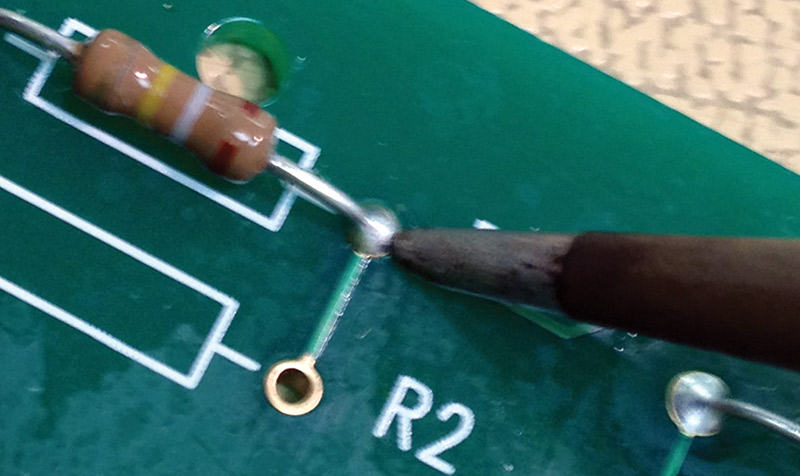
FIGURE 5. Choosing the right tip, which is 50%-75% of the pad size.
If a tip that is too small is used, you will not be able to transfer the necessary heat needed to form the solder joint quickly (about 2-3 seconds). If a tip is too large, you may damage the laminate of the board around the area being soldered. This is why it is so important to choose the correct tip size. A “near fit” is not good enough for most applications. When soldering, contact both the lead and the pad simultaneously. This — in conjunction with a properly formed heat bridge — will allow you to quickly solder the part.
Before and after soldering, it is important to clean and inspect the solder joint. For a solder joint to be properly formed, the connection area and lead must be clean and free of any foreign materials. After soldering is completed, all flux residues should be removed from each solder connection by cleaning with isopropyl alcohol or another cleaning agent, and then blotting the area dry with a lint-free ESD safe tissue. Not doing so may leave you something that looks like Figure 6, and it could interfere with a good solder joint.
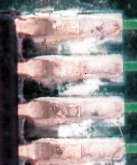
FIGURE 6. Flux residue between QFP leads.
The completed assembly should be totally free of flux and residual cleaning agents. Unless you are using “no clean” solder, always remember that the first and last step of the soldering process is cleaning.
In appearance, solder joints may have from a shiny to satin luster and generally smooth appearance. Lead-free solders may have a slight grainy surface. The solder filet should be concave in shape. Generally, however, touch-up (rework) of soldered joints should be performed only when the reliability needs to be improved to avoid causing added problems by the introduction of additional heat.
Terms
Before we end this part of the guide, there are some common terms utilized in electronics assembly that will be used going forward that are important to understand.
Component — A component refers to any device that handles electricity.
Leads — Many components have leads, which are two or more rigid metal wires which stick out of the component. Some leads are straight, some are not. Some leads are made of round wire, others are made of flat wire.
Through-hole Components — Components with leads (Figure 7) that are meant to be soldered through holes in the board are known as through-hole components. We will talk more about leads later on when we talk about soldering specific parts.
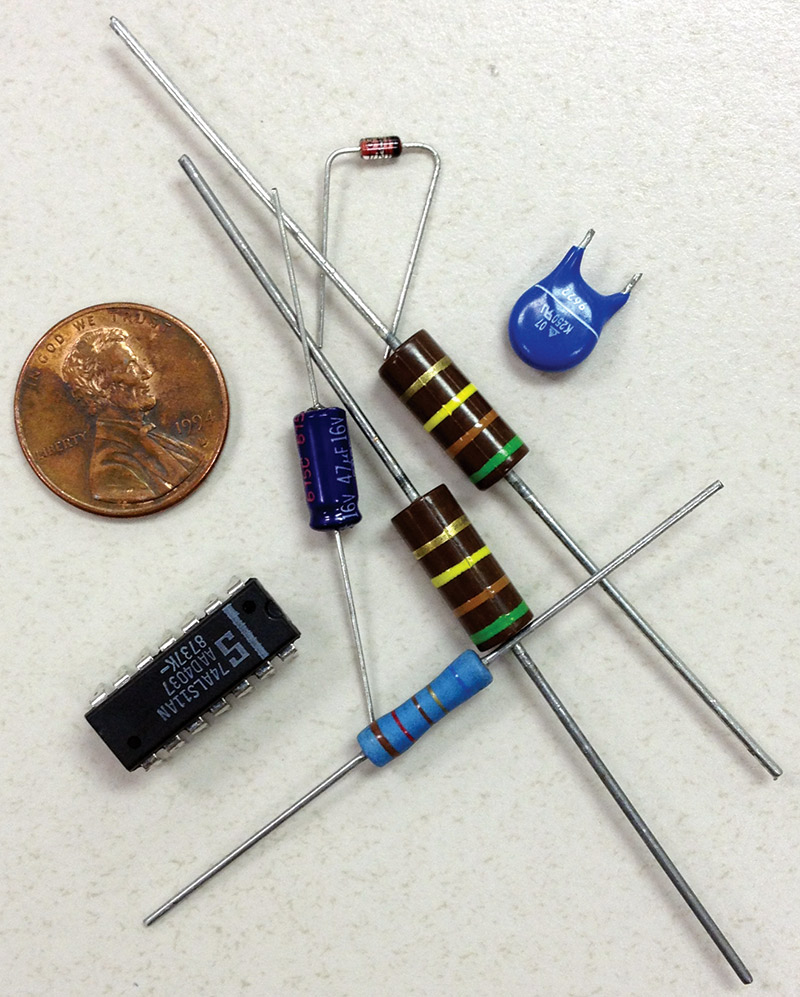
FIGURE 7. Through-hole components.
Surface Mount Devices (SMD) — As designers have increased the density of parts on a PCB (printed circuit board), component sizes have correspondingly shrunk in physical size. Components commonly have their electrical connections to the PCB on the underside of the component body in order to reduce the footprint. These components are attached to the surface of the printed circuit board with solder. Surface mount components are usually called SMDs (surface-mount devices — Figure 8) for short.
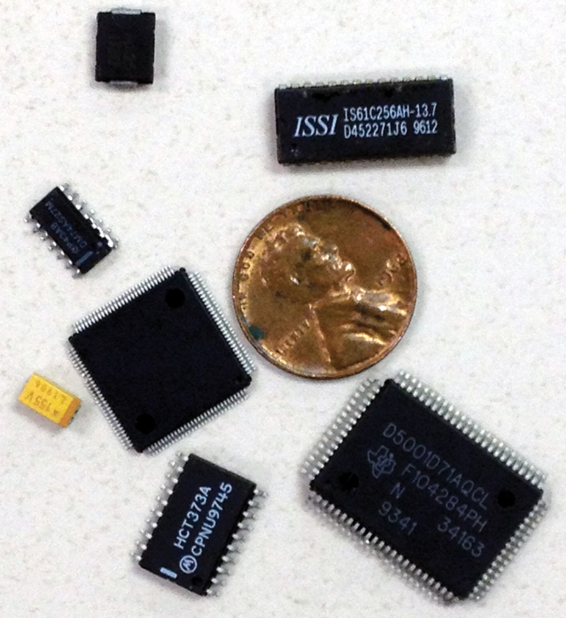
FIGURE 8. SMT components.
Polarity — Also keep in mind that some components — such as diodes — have a positive and negative connection to the board, and so must be placed on the board with the connections oriented properly. Components with positive and negative connections are said to have polarity. The positive lead is called the anode, while the negative lead is called the cathode. Polarity can be indicated on parts in a variety of ways, including (+) and (-) symbols. Markings and symbols for either the anode or cathode leads can take many shapes and forms.
Value — Some components will also have a value, which is a numerical quantity given to them, and a tolerance which is the variation from the value allowed for that component. Resistors and capacitors are common components on PCBs and it is critical that the right valued components (many of which look exactly the same physically) are placed in the correct location on the PCB.
Orientation — Another thing to keep in mind when placing components is orientation. Component orientation refers to how the component is to be positioned and soldered to the board. Orientation is usually marked in some way on the component’s body. Orientation marks (Figure 9) — or symbols — include: a notch, a dimple, a wedge, a stripe, or numbers.
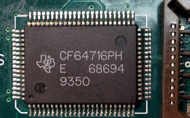
FIGURE 9. Proper orientation is important on certain components. Be sure to match it to the board.
With multi-pin components such as ICs, these orientation symbols indicate where “pin 1” of that component is located, so that pin may be mated with the corresponding pad or land on the board. Matching orientation marks may be found on the board. These include a symbol — usually a plus — and/or a square pad or land on the board.
Next in this series, we’ll discuss soldering through-hole components like connectors, so stay tuned. SV
Article Comments