The Biggest and Smallest 555 You’ll Ever See!
By David Goodsell View In Digital Edition
I have a shelf in my office where I display my treasures, old and new. There are some neat 3D printed parts, old Nixie tubes, and a vintage HP35 RPN calculator. I just added a new plaything to my collection: the discrete 555 timer from the Evil Mad Scientist Laboratories.
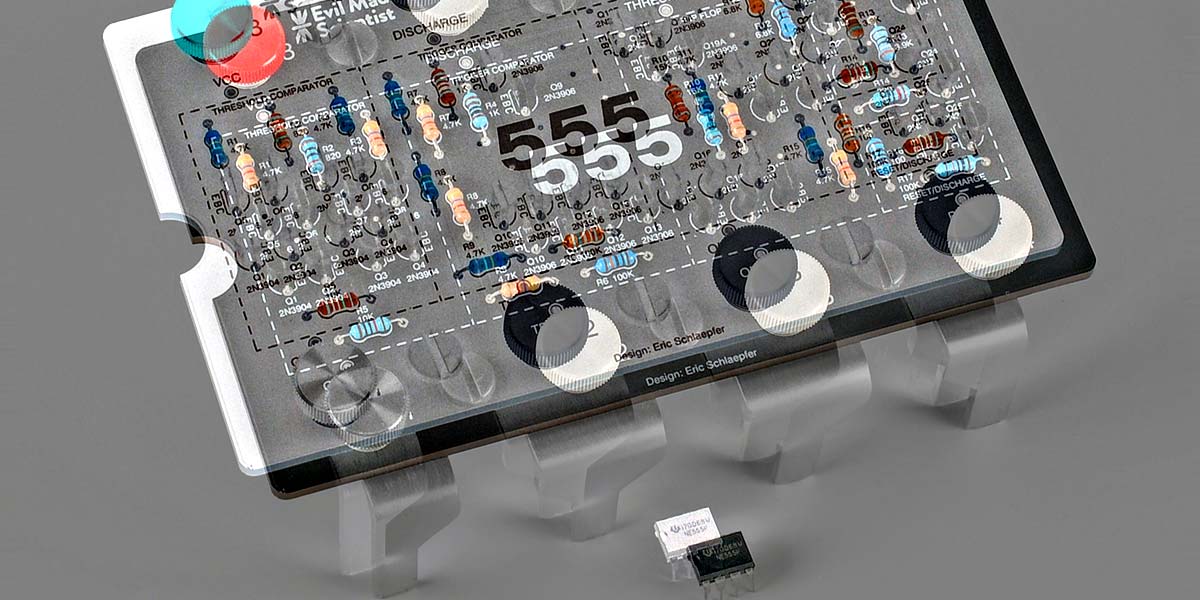
Figure 1 shows the Discrete 555 Timer Kit designed by Eric Schlaepfer (https://shop.evilmadscientist.com/productsmenu/652). It replaces all the integrated components in the smaller IC version with much larger discrete through-hole parts. Included are 13 2N3904s, 13 2N3906s, 17 resistors, and a board that is A WHOLE LOT BIGGER than the normal die inside a 555 IC — all for $35.
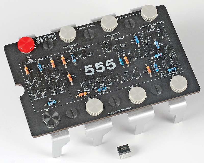
FIGURE 1. The giant “discrete 555 timer” soldering kit replicates the integrated circuitry in the smaller DIP version.
The quality of the circuit board is excellent, and it went together without a hitch. The electrical connections are made through eight knurled knobs instead of the handsome aluminum “pins” which act as legs for the board. All in all, it’s a classy piece of work.
After finishing the kit, I cobbled together a little flashing LED circuit to see if it would actually work like the real thing. Blink, blink, blink it went. Success! I found a prominent place on my treasure shelf and it has since impressed everyone who has seen it. Of course, someone had to ask, “It sure looks nice, but what is it good for?” So, I wracked my brain for a suitable application. Figure 2 is the light-hearted result.
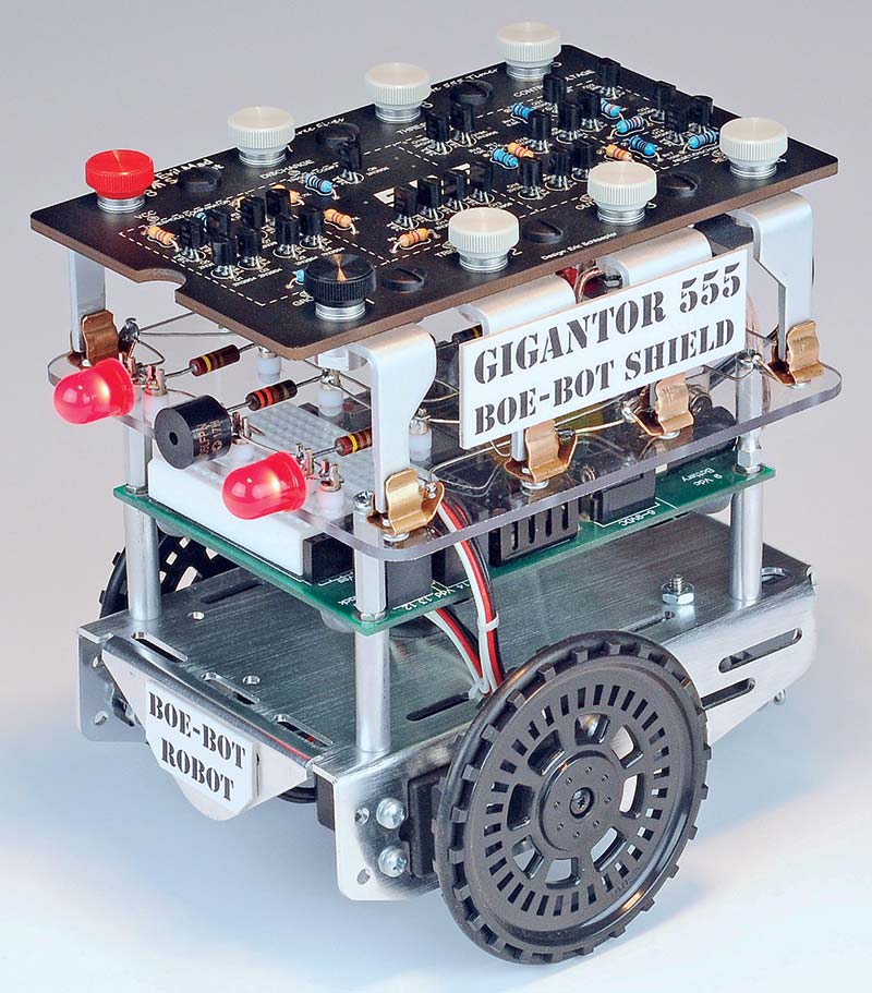
FIGURE 2. The Gigantor 555 Shield ushers in a new era of robotic safety with warning LEDs and beeper.
THE GIGANTOR 555
I’d like to introduce you to the revolutionary GIGANTOR 555 Boe-Bot Shield. I designed the shield to use with Parallax’s famous educational robot. It only has nine components, but adds a very important capability to the Boe-Bot. The shield flashes two jumbo LEDs and a beeper which act as warning signals to young children and small pets who may be in the path of the oncoming robot. Check out the diagram in Figure 3.
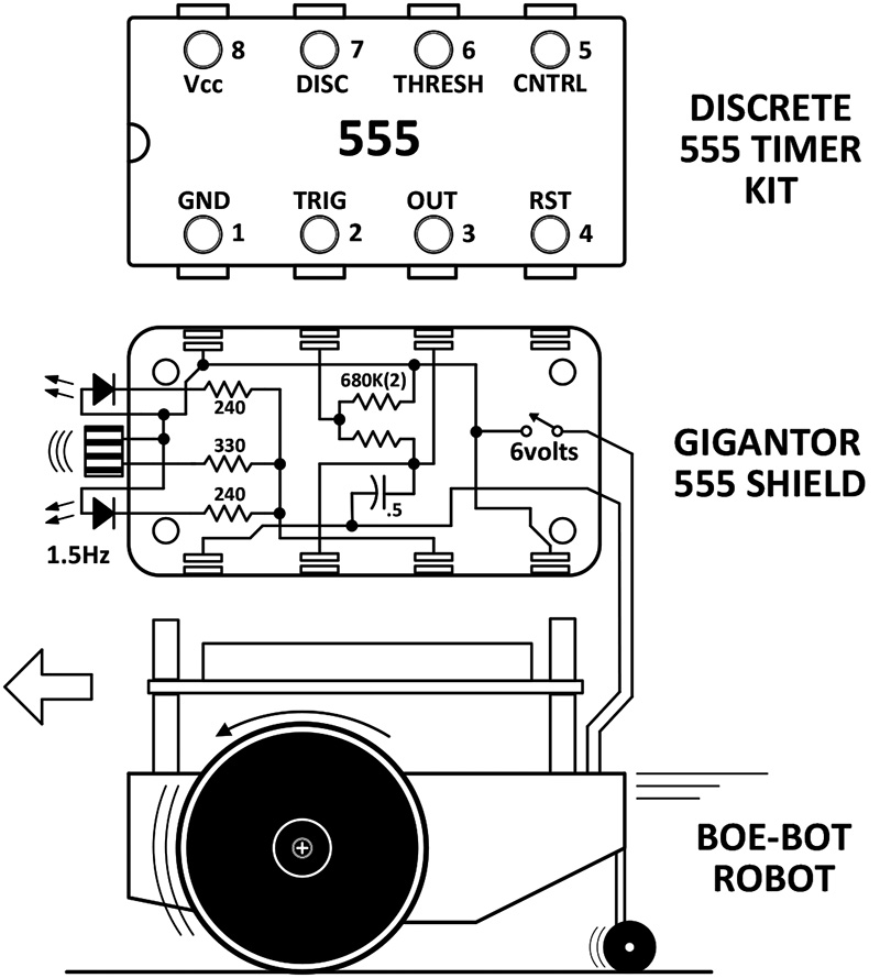
FIGURE 3. The discrete 555 timer mates with the shield using modified fuse clips.
As you know, I could have used a $0.50 555 IC to flash the LEDs, but I was desperate to find an application for my new 555 timer board. So, I mated it to the shield with some old fuse clips. Figure 4 shows the Gigantor patrolling the house.
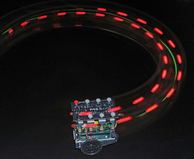
FIGURE 4. Autonomous Gigantor robot on patrol.
I did make one mechanical change to the legs in the kit to make them compatible with the shield. I cut the left and right legs apart into eight separate “pins,” then connected each one to its respective electrical post. This allowed the modified pins to electrically mate with the clips below (see Figure 5).
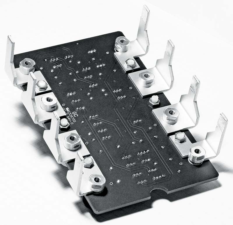
FIGURE 5. The eight modified legs are fastened to the board with custom nuts. The non-conductive anodizing was removed from the tips to connect with socket clips.
A NEW PERSPECTIVE
While the kit was fun to build, there was another aspect of the 555 that I thought you might enjoy learning about. A while ago, an inquisitive software engineer named Ken Shirriff decided to look at the 555 from a completely different perspective, i.e., microscopically. He took detailed high-magnification photos of the various integrated structures on an actual 555 silicon die using a special microscope and explained the technical operation of many of the functions on the chip. A link to his webpage and blog can be found in the sidebar.
1. See “Ken Shirriff’s Blog” at www.righto.com for his humongous site covering many interesting projects.
2. www.righto.com/2016/02/555-timer-teardown-inside-worlds-most.html
Ken has graciously given me permission to use his microphotographs to illustrate how the various components such as transistors and resistors are constructed on the die. I’ve taken the liberty of adding some annotations to his photographs to help explain them.
However, I’m not going to delve into the operation of the 555 because it has been covered extensively in other places. My focus will be mostly on the visual.
THE BIG REVEAL
First, Figure 6 shows the metal can version of a bipolar 555 with its top hacked off, compared to a penny. The little rectangular silicon die is in the center of the can and is about 0.063”wide, which is 1/16 of an inch. Pretty small.
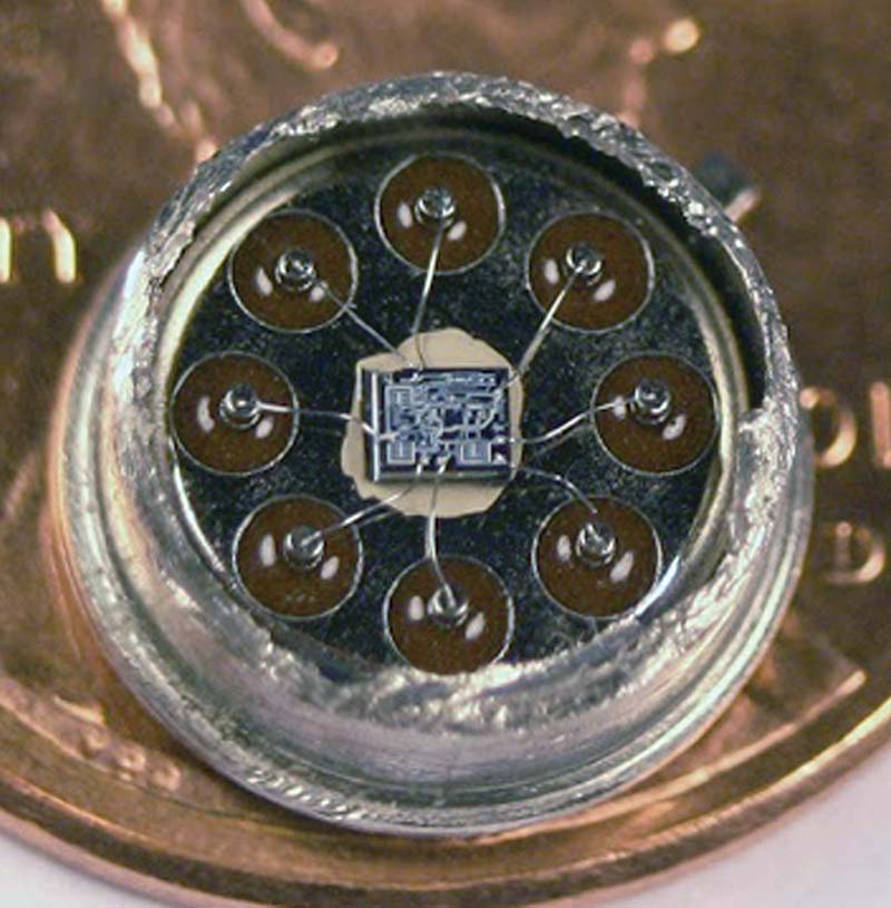
FIGURE 6. Inside the metal can version of the 555 is the tiny integrated circuit chip, connected to the pins with eight thin wires.
Figure 7 is the big reveal: a highly magnified color-annotated view of the entire die. The black leads around the outside are the eight wires that connect the pads on the die to the pins of the package. The yellowish lines are deposited metallization traces that are the same as the wires on a printed circuit board (PCB).
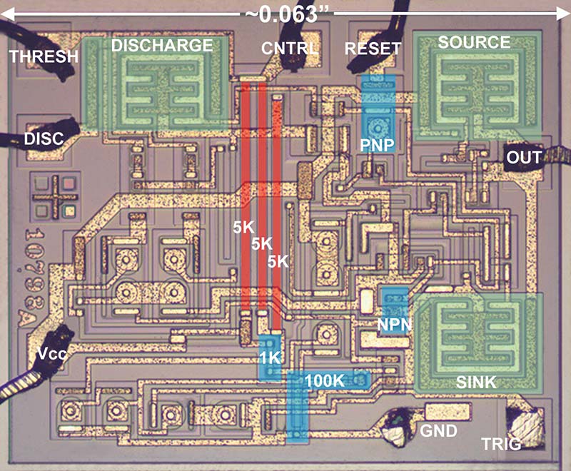
FIGURE 7. A magnified view of the die (chip) shows 41 components interconnected by the yellowish metallization layer.
Since there are more than three dozen transistors and resistors on the die, I have selected just a few to focus on. Most major types of components are very similar throughout the chip, although in some cases, you have to examine them closely to see the similarities. Figure 8 is the schematic and is color-coded the same as Figure 7, so you can discern which components are which. Keep in mind that the discrete 555 timer board used in the Gigantor may have slightly different resistor values for various reasons.
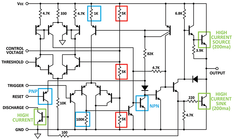
FIGURE 8. The colored boxes on the schematic show the locations of the same components that are color-tinted in Figure 6.
THE RESISTORS
Referring back to the big picture of the die in Figure 7, the simplest resistor is the tinted-blue 1K version in the lower middle. Figure 9 is a super close-up view of its structure. The actual resistor is the faint bone-shaped outline of P-type silicon that has been deposited between two pads.
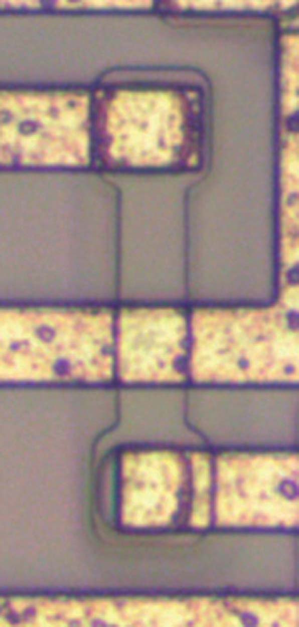
FIGURE 9. In this highly magnified view, the simplest resistor is a 1K dog bone shaped structure.
Notice that another wire passes directly through the middle of the resistor. This doesn’t matter because a thin layer of transparent non-conductive silicon dioxide (SiO2) has been deposited underneath the crossover wire, so it doesn’t make contact with the resistor below. Pretty clever.
A more complicated L-shaped resistor structure called a “pinch resistor” is seen in Figure 10. Higher value resistors (like 100K) can be made by depositing a second thin layer of N-type silicon on top of a regular resistor. According to Ken, “This makes the conductive region much thinner (i.e., pinches it), forming a much higher but less accurate resistance.”
FIGURE 10. This 100K L-shaped resistor uses an overlay of N silicon to create a “pinching” effect to attain its high resistance.
THE MAGIC 5K + 5K + 5K DIVIDER
Looking back at Figure 7 once again, the most interesting resistors on the chip are the three 5K vertical strips (tinted red for clarity) in the center. They are also located in the center of the Figure 8 schematic. Notice that the three resistors are in series, and form the critical 1/3, 2/3 divider that sets the reference voltage points where the external capacitor charges and discharges.
The magic of them is that the 1/3, 2/3 ratio remains constant over the full range of Vcc, and therefore any changes in the supply voltage have no effect on the timing cycle. Only the values of the external resistors and capacitor dictate the charge/discharge timing.
There’s an interesting aspect regarding the 555 name. Ken’s blog says, “Urban legend says that the 555 is named after these three 5K resistors, but according to its designer, Hans Camenzind, 555 is just an arbitrary number in the 500 chip series.”
TRANSISTORS COME IN DIFFERENT SHAPES
The last things I’m going to cover are the bipolar transistors: NPN, PNP, and high current, shown in Figures 11, 12 and 13, respectively. I’m using Ken’s graphics to show the complexities and differences between NPN and PNP structures.
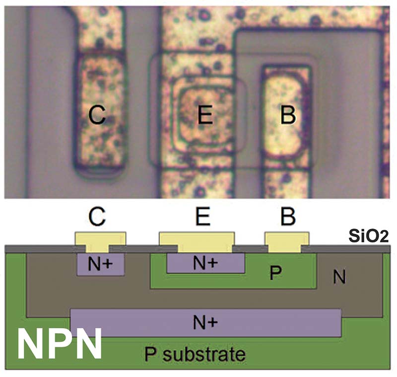
FIGURE 11. Integrated transistors are constructed of several layers; the base of this NPN one is not in the center as you might expect.
In the Figure 11 NPN transistor, the emitter is the bullseye pattern in the center, with the offset rectangle of P material forming the base. Normally, we think of a transistor as a stack of three layers like N-P-N, but in the case of integrated circuits, the structures are more complex. However, you can still see that the yellow-colored metallization is connected to an N+ region, P region, and another N+ region, NPN. Some of the buried layers serve to isolate it from neighboring components.
PNP transistors are completely different, as seen in Figure 12. If you follow the yellow metallization connections, the circular emitter is touching a P region, the base is N+, and the collector is connected to a P material. Ken’s explanation is, “Although the metal contact for the base is on the edge of the transistor, it’s electrically connected through the N and N+ region to its active ring in between the collector and emitter. A metal line is routed between the collector and base, but is not part of the transistor.” A thin layer of SiO2 insulates the metal line from the N material below.
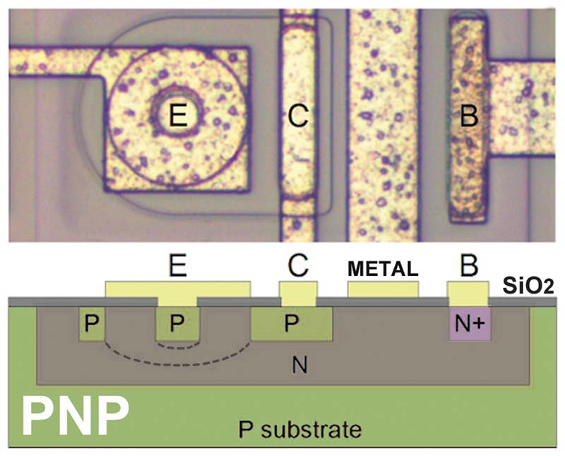
FIGURE 12. The PNP transistors are unlike the NPN units and can be identified by their circular feature.
The largest structures on the chip are the three high-current NPN transistors, magnified in Figure 13.
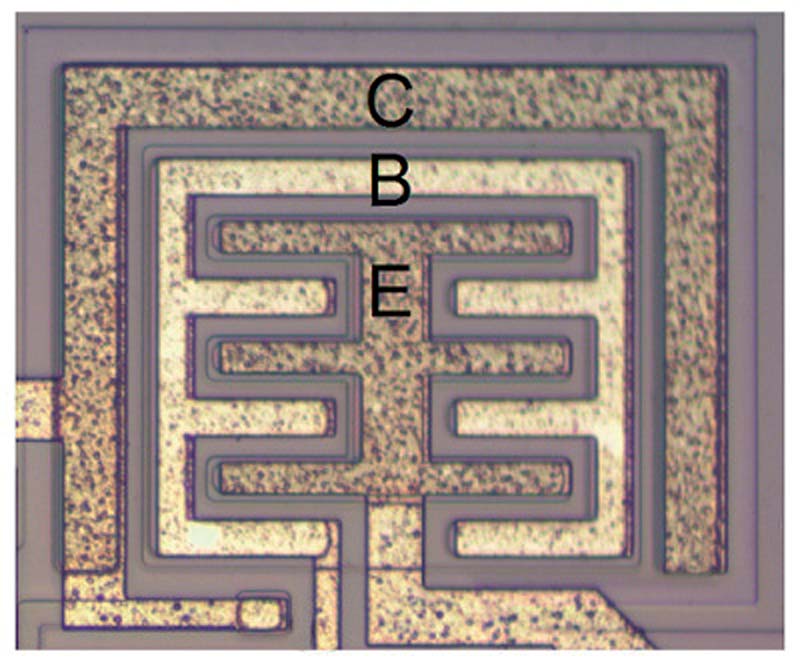
FIGURE 13. Three high current (200 mA) NPN transistors are used to discharge the external capacitor and drive the 555’s output.
The structure is more classic looking, with interlocking fingers for the emitter and base surrounded by a large three-sided collector. In the schematic (Figure 8), the high current one on the left is used to discharge the external timing capacitor and the other two provide 200 milliamp source and sink capabilities for the output.
Well ... that’s about it for the die.
IN CLOSING
My intent in this article was to briefly show you some of the interesting structures in a bipolar 555. For more detailed information, please see Ken’s blog where he covers the current mirrors, differential pairs, and some of the development history of the 555.
The GIGANTOR 555 Shield was a one-off affair, designed to show that even a giant 555 board could be somewhat useful. However, I doubt that the discrete board will replace the current DIP or SOIC versions, but it does illustrate just how complicated integrated circuitry can be. SV
Parts List
| ITEM | DESCRIPTION | SUPPLIER |
|---|---|---|
| C1 | Capacitor, 0.47 or 0.5 µF, 50V | Jameco #2236973 |
| R1, R2 | Resistor, 240 ohms | Jameco #661351 |
| R3 | Resistor, 330 ohms | Jameco #661386 |
| R4, R5 | Resistor, 680K | Jameco #691542 |
| SW1 | Switch, Toggle, SPST | Jameco #317228 |
| LED1, LED2 | LED, Red, Jumbo size | Jameco #2152155 |
| BP1 | Beeper, 4-7V | Jameco #76065 |
| ROBOT | Boe-Bot Robot Kit | Parallax #28832 |
| TIMER | Discrete 555 Timer Kit | Evil Mad Scientist #555 |
Article Comments