The Basics of Soldering — Part 4
By Bob Wettermann, Nick Brucks View In Digital Edition
After discussing both leaded as well as SMT (surface-mount technology) soldering, we come to the final installment of this series where we’ll cover advanced SMT package soldering.
Ball grid arrays (BGAs) are a type of SMT package for integrated circuits that attach to the board using a grid of solder balls on the underside of the component. This allows for a large number of leads to make contact with a very small area of a printed circuit board (PCB), even compared to the most densely packed DIPs (dual in-line packages) and SOICs (small outline integrated circuits).
In the electronics industry where miniaturization is key, this package style has proven easy to place with manufacturing equipment and has also been proven to be very robust in terms of longevity.
On the other hand, leadless devices — common types include QFNs [quad flat no leads] and LGA [land grid array] package styles — pursue miniaturization through a different route. Rather than attach to the board with any extended legs or leads, these devices make contact using solder “bumps” on the bottom of the component package.
The place you will most often see these types of SMTs will be where very flat structure heights are required, such as in handheld devices or where a lot of heat dissipation is necessary.
However, the price of this compactness is that both of these component types are consequently difficult to place for hobbyists for single devices when there is no stencil printing involved. In addition, these packages generally require capital intensive/precision machines in order for them to be placed consistently.
Because of this, instead of focusing on the initial placement of these components using the print and place process, this guide will instead turn an eye towards the hand prototype placement of such components.
Materials needed include:
- Stencils
- Solder paste
- Isopropyl alcohol and lint free wipes for cleaning the stencil
- Solder wick
- Miniature squeegee
- Reflow source — either a heat gun or a reflow oven
As always, remember to take the necessary ESD and safety precautions to avoid any potential hazards to you or to the components mentioned throughout this series.
Let’s start with leadless component repair. Once you’ve picked up the part, you'll want to use a QFN stencil to place the bumps on the bottom of the component, since doing this manually is time-consuming and difficult to be accomplished at an even height — even for trained technicians.
To get started, clean off contaminates on the lands of the device.
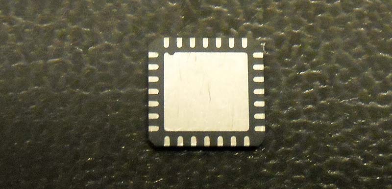
Figure 1. The removed device.
Place the larger of the two stencils, with the part lands properly aligned with the apertures of the stencil.
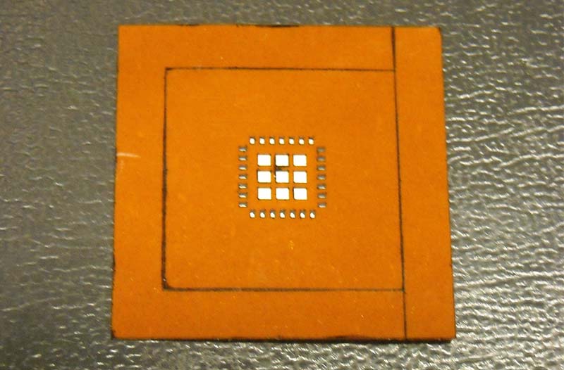
Figure 2. Make sure the apertures of the stencil are properly aligned on the part.
Squeegee solder paste into the apertures of the stencil. Using the squeegee, scoop a little solder paste out of the container, then starting at one side roll solder paste into the apertures by moving the squeegee to the opposite side of the stencil.
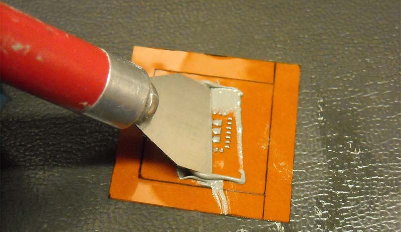
Figure 3. Don't worry if there's a little excess paste on the stencil. It can be easily wiped off with a lint free cloth.
After wiping off any excess solder, reflow based on the type of solder you are using. It is recommended that this be done by running the assembly through a reflow oven (toaster oven with controls will work). However, a heat gun can also suffice.
Remove the stencil from the device and clean off the part lands using isopropyl alcohol. You should see uniform and consistent solder bumps on the lands.
Now, prepare the board that the device will be placed on by using isopropyl alcohol.
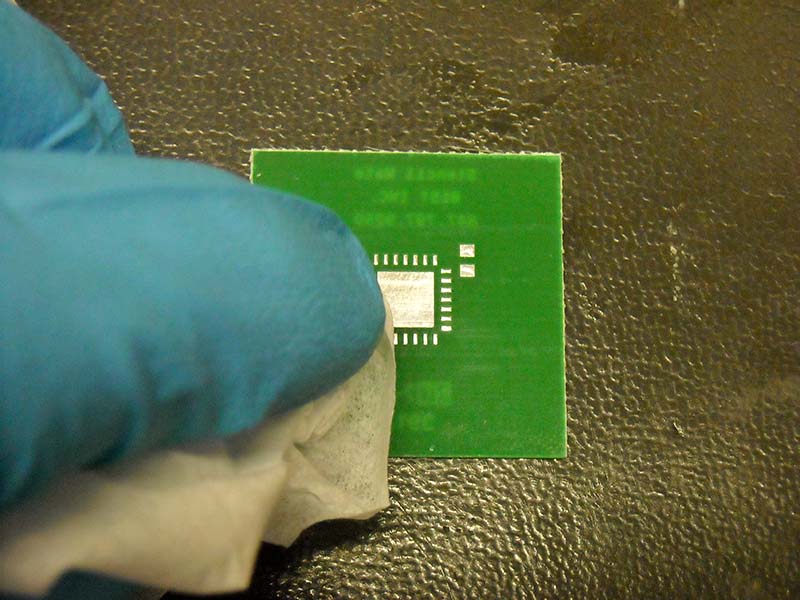
Figure 4. If using a brush to apply alcohol, be careful not to scratch the PCB.
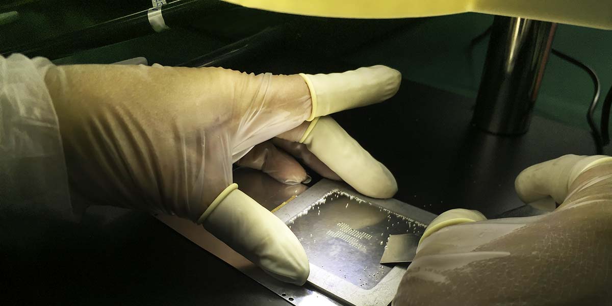
Place the board stencil onto the PCB. We used a StencilMate™. Once it is properly aligned, apply pressure to the stencil to stick it in place in order to activate the adhesive. Make sure that the apertures line up with the lands before you do this because once the stencil is stuck down, it cannot be removed and reused. To make any changes after this point, you will have to start over.
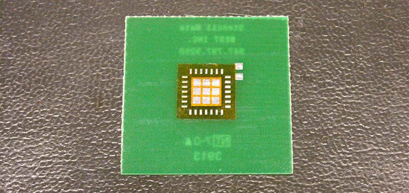
Figure 5. Make sure that the apertures are well aligned before you fully stick the stencil down.
As before, squeegee solder paste into the stencil.
Place the bumped device into the stencil. Reflow again using the same profile to reflow the solder paste.
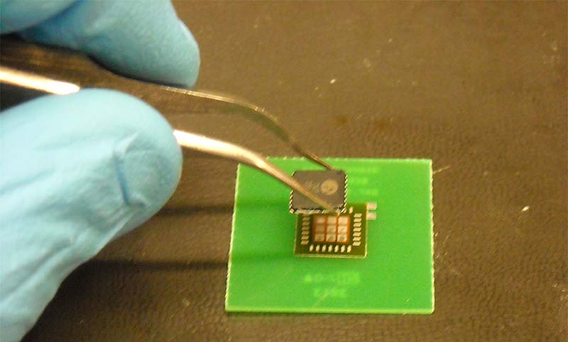
Figure 6. Generally, you'll want to place these components with tweezers due to their small size.
Inspect the final product for any anomalies. Make sure that the part lies flat and hasn’t been damaged in any way by the heat. Unfortunately, due to the nature of the leads of the component, inspecting the underside to check for good solder contact is difficult. Often, the only way to truly know if it works is to test it.
When it comes to placing BGAs, the main issue you will see is the problem of placing fine-pitched devices and having solder joints which cannot be visibly inspected from the solder ball to the land.
Clean the site using isopropyl alcohol to get rid of any contaminants that might interfere with a good solder joint.
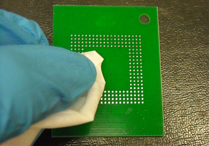
Figure 7. A good rule is to clean any PCB or component before soldering it since it is much easier to clean something with alcohol than it is to remove and replace a part because oils or contaminants interfered with the solder making good contact.
Peel the adhesive backing off of the stencil.
Align the stencil. The most reliable way to do this is to line up diagonally opposite corner apertures over their corresponding lands.
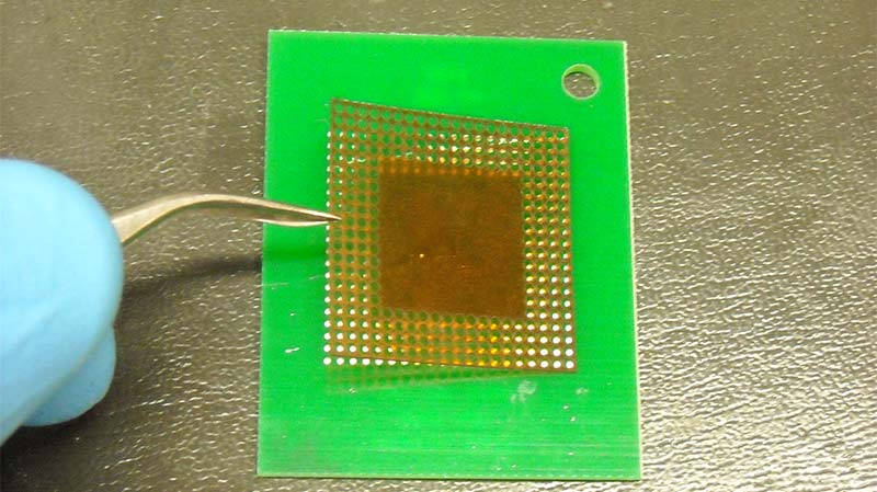
Figure 8. As with the leadless device, tweezers are very useful in placing stencils and components on a PCB.
Once you’re sure the stencil is well aligned, place the stencil starting at one corner and slowly work towards the opposite corner. Smooth down the stencil afterwards to remove any air bubbles. Apply pressure to activate the adhesive.
Squeegee solder paste across the top of the stencil. Make sure paste has been rolled into all of the apertures.
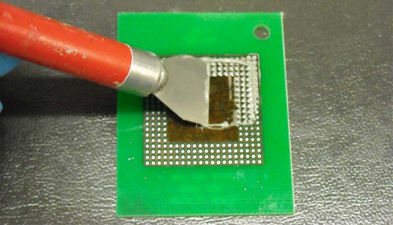
Figure 9. As you did before, roll solder paste into the stencil.
Wipe off any excess solder paste on top of the stencil using a lint free wipe.
Gently place the BGA. Make sure the balls or leads of the component of the part are aligned with the apertures.
Reflow the part either using a toaster oven or a heat gun.
Inspect the BGA to make sure it is level and look under the component to ensure that none of the solder balls are cracked or bridged in any way.
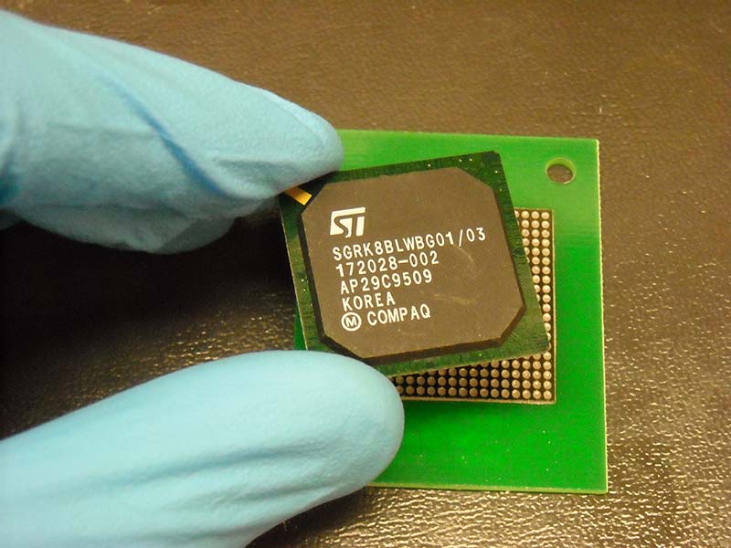
Figure 10. For a part of this size, it is most likely easier to just place it by hand rather than with tweezers.
Through this series of articles, we hope you’ve acquired a few new skills to help you in your projects. These guides should at least provide a solid base on which to build more advanced soldering skills, or simply to do a little rework or repair from time to time. Regardless of what you choose to use these skills towards, we trust you have learned something of value. SV
Article Comments